














LG’s New FLiPP OLED Tech Promises Brighter, Longer-Lasting Screens
LG Display unveils FLiPP, a next-gen OLED manufacturing method that eliminates metal masks to deliver 1.6x brighter screens and 2.4x longer lifespans.


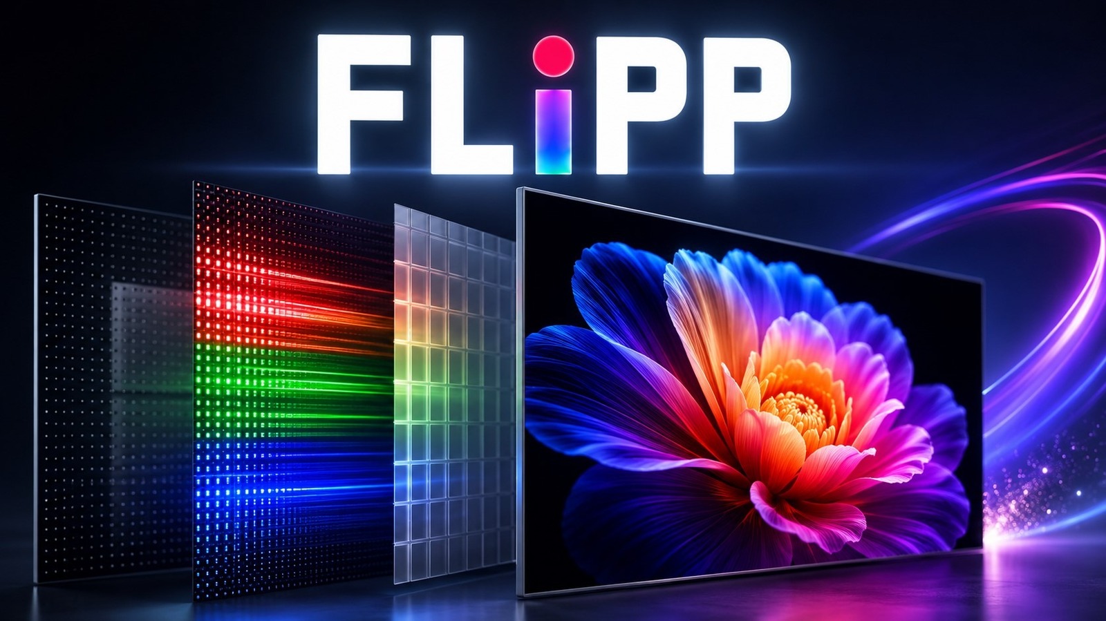
Tech giant LG Display unveils a groundbreaking manufacturing process for organic light-emitting diode (OLED) screens, promising a massive leap forward in display performance and scalability. Dubbed FMM-Less innovative Pixel Patterning, or FLiPP, this new production method eliminates long-standing manufacturing bottlenecks to create panels that are brighter, more durable, and highly energy-efficient. The announcement marks a major milestone in display engineering, offering a versatile solution that can scale to virtually any screen size.
At the heart of this innovation is the complete removal of the traditional fine metal mask, a stencil-like component historically used to deposit red, green, and blue pixels onto a substrate. Instead of relying on this physical template, the new technique arranges the primary colors sequentially and employs advanced photolithography alongside ultraviolet light to precisely etch away unwanted materials. This shift in fabrication yields staggering performance improvements, including a 60 percent increase in peak brightness and a lifespan that is nearly two and a half times longer. Furthermore, the streamlined pixel architecture reduces overall power consumption by 13 percent.
For years, the display industry has struggled with the physical limitations of the fine metal mask process. As screen sizes increase, these thin metal stencils are prone to sagging under their own weight, which leads to pixel misalignment and high manufacturing defect rates. This physical vulnerability has historically limited the cost-effective production of very large OLED screens while also restricting the pixel density required for ultra-high-resolution micro-displays. By bypassing the physical mask entirely, the new photolithography-based method removes these physical barriers.
Industry analysts view the integration of semiconductor-grade photolithography into display manufacturing as a logical evolution that bridges the gap between microchips and screens. This crossover technology is particularly crucial for the burgeoning virtual and augmented reality markets, where displays must pack thousands of pixels into a space the size of a postage stamp without sacrificing brightness. While competitors scramble to improve traditional masking techniques, this shift to a mask-free optical patterning system establishes a new benchmark for high-density pixel alignment.
The implications of this technological leap extend far beyond mere specification sheets, directly addressing the most common consumer complaints regarding OLED technology. Increased durability directly combats the dreaded phenomenon of screen burn-in, while the enhanced energy efficiency translates to longer battery life for portable devices. Manufacturers also gain unprecedented design freedom, as they can now engineer displays with custom shapes and ultra-thin profiles that were previously impossible to manufacture reliably. This versatility ensures that future consumer electronics will look better and last longer.
Looking ahead, the initial rollout of this next-generation display technology will target mid-
Originally reported by The Verge
What's Your Reaction?
 Like
0
Like
0
 Dislike
0
Dislike
0
 Love
0
Love
0
 Funny
0
Funny
0
 Angry
0
Angry
0
 Sad
0
Sad
0
 Wow
0
Wow
0